


- Die & Wafer
- +Supplier Line Card
- Alliance Memory
- Analog Devices
- Apogee Semiconductor
- Analog Power
- Avalanche Technology
- Central Semiconductor
- Diodes Incorporated
- Cypress
- Everspin Technologies
- Interfet
- International Rectifier
- ISOCOM Limited
- ISSI
- Knowles
- Linear Integrated Systems
- MACOM Technology
- Microchip
- Micron Technology
- NXP Semiconductors
- On Semi
- Renesas
- Samsung Semiconductors
- SemiQ Inc.
- Semicoa
- Texas Instruments
- Transys
- Vishay
- VPT Components
- +Quick Turn Services
- –Wafer Processing
- +EOL/DMSMS Sustainment
- +Component Design & Packaging
- Advanced Interconnect Technologies
- 2.5 & 3D Heterogeneous Integration
- System in Package (SiP)
- Multi-Chip Modules (MCMs)
- Wafer Bumping & WLP
- Design, Packaging & Assembly
- Assembly Services
- Chip on Board (CoB)
- Plastic Packaging (BGA/CSP/QFN)
- Hermetic Packaging
- OSAT Services
- +Supplier Line Card
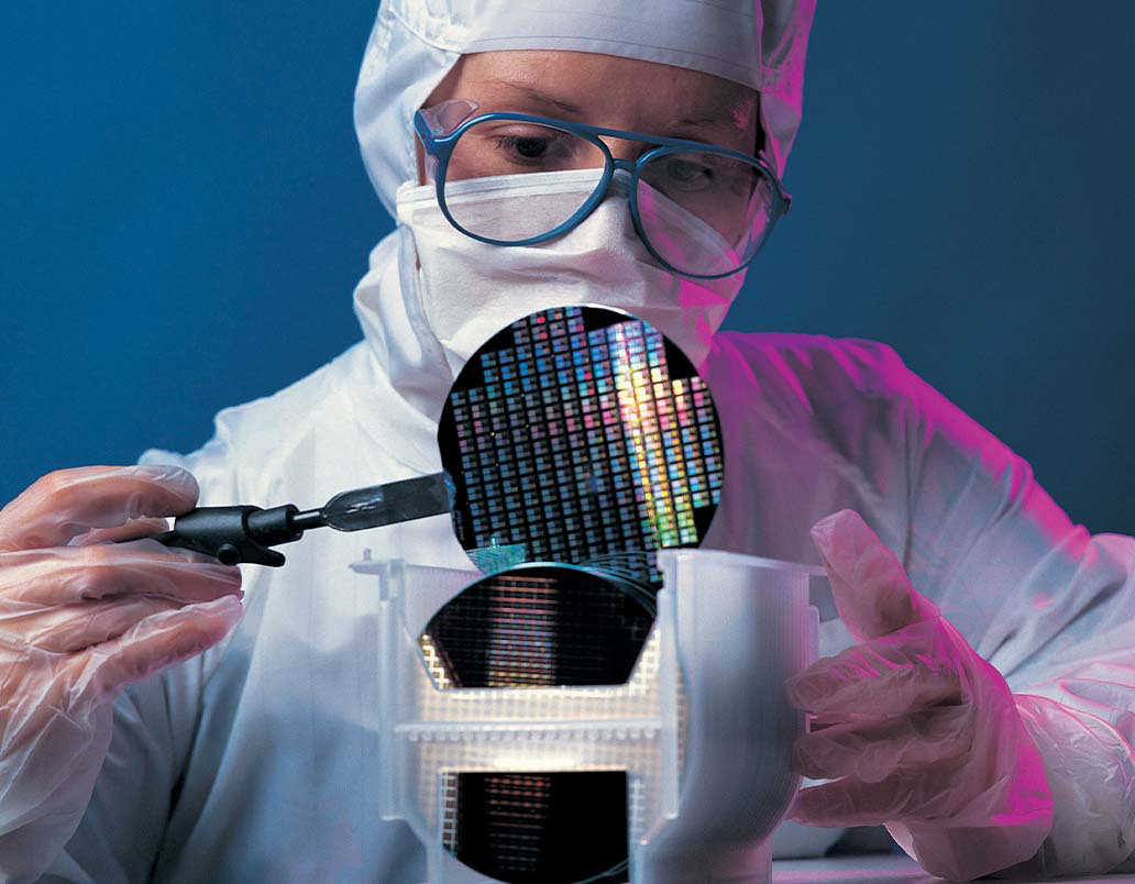
One Source, One Solution for your Bare Die and Wafer needs
Micross is the largest worldwide value-added bare die processor and distributor with a comprehensive array of capabilities to fully process wafers; from wafer saw to wafer bumping for your entire bill of materials. Whether a commercial product or your own die design, we will process wafer product to your exact specifications and choice of end supply form.
Over the years, Micross has developed and maintained key relationships with many of the leading semiconductor manufacturers providing us with the capability to offer an extensive bare die portfolio to our customers.
The Micross Advantage
Manufactured wafers must be handled both carefully, to avoid damaging valuable circuits. and quickly, to shorten the time to value. During three decades of working to the stringent requirements of military and aerospace companies, Micross has developed a quality assurance program that is second to none. Now commercial companies as well can benefit from Micross's full range of die processing services.
- More than three decades of experience serving commercial, military, and aerospace markets
- Custom die processing operations to the most stringent specifications
- Integrated operations for fast time-to-market
- Guaranteed first-time success
Capabilities
- Wafer sawing up to 300 mm (12 inches)
- Silicon and non-silicon materials
- Automated and manual pick and place
- Automated and visual inspection
Downloads & Resources
Wafer Thinning & Dicing
Wafers thinned down to 100µm, dicing of wafer sizes up to and including 12” (300mm)
More infoDie Plating / Customized Output
Automated, virtually contactless handling of singulated die, multiple bin/grade die picking
More infoVisual Inspection
Acceptable Quality Level (AQL), MIL-STD, inspection via AOI equipment available, up-to-date automatic inspection equipment
More infoLot Acceptance Testing
Conversion between industry formats, inking using any electronic wafer map
More info