


- Advanced Interconnect Technologies
- 2.5 & 3D Heterogeneous Integration
- System in Package (SiP)
- Wafer Bumping & WLP
- Multi-Chip Modules (MCMs)
- Novel Microfabrication & MEMS
- Design, Packaging & Assembly
- Assembly Services
- Final Test
- Chip on Board (CoB)
- Plastic Packaging (BGA/CSP/QFN)
- Hermetic Packaging
- MIL-STD-1553 Data Bus Couplers & Accessories
- Micro In-Line Couplers
- Tab Mounted In-Line Couplers
- Through Hole Mounted In-Line Couplers
- Box Couplers
- Custom Design Couplers
- Data Bus Coupling Transformers
- Data Bus Relays
- Data Bus Harnesses
- Bus and Stub Terminators
- Wide Bandwidth RF & Video Transformers
- Antenna Couplers
- Video Isolation Transformers
- RF Wideband Transformers
- RF Wideband Transformers & Impedance Adapters
Micross Advanced Interconnect Technology (Micross AIT) is home to one of the premier wafer bumping and wafer level packaging facilities in the U.S., with 20+ years of experience in developing and providing leading edge interconnect and integration technologies to customers around the world. We have the unique ability to support early stage development needs as well as low-to-mid volume production for more mature applications. Our ITAR Registered facility supports wafer sizes up to 200mm with established and proven WLP processes and the flexibility to tailor unique solutions for your most demanding interconnect requirements.
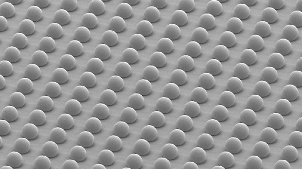
Solder Bumping and Wafer Level Chip Scale Packaging
Micross AIT provides full in-house state-of-the-art wafer bumping and WLCSP solutions. Whether you have a need to process a single wafer or are looking for a source to provide recurring production services, Micross AIT has a wide array of WLP technologies.
- WLCSP ball place, electroplated C4, and Cu pillar bumping with bump diameters as small as 25 microns
- Bump-on-pad and bump-on-polymer processes
- Single and multiple layer Cu redistribution with several polymer repassivation material choices
- Eutectic Sn/Pb, Pb-free and high-Pb solder alloys
- Design services and custom test vehicle fabrication